- Get in Touch with Us
Last Updated: Apr 25, 2025 | Study Period: 2022-2030
A wafer is a piece of semiconductor material that is shaped like a very thin disc and made of silicon, one of the most prevalent semiconductors in use today.
Silicon-based photovoltaic cells and electronic integrated circuits (ICs) are both made from wafers. The wafer acts as the substrate in these designs.

The most common size for silicon wafers used in the production of solar cells is 125mm. Typically, a single solar cell will require a wafer of 10 meters. Larger 125mm silicon-based wafers, however, can be up to five times bigger.
The global 125mm wafers shippers market accounted for $XX Billion in 2021 and is anticipated to reach $XX Billion by 2030, registering a CAGR of XX% from 2022 to 2030.
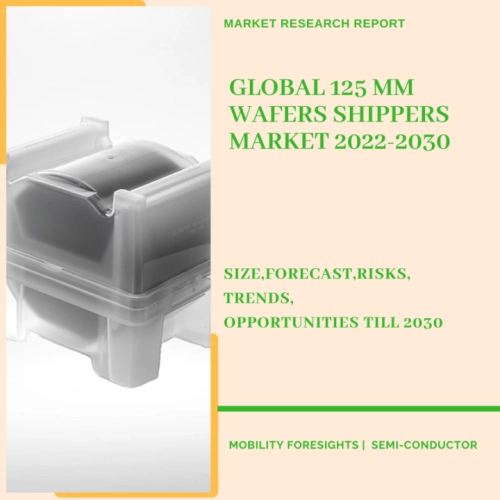
Introduction of 125 mm Wafer Shippers by Entegris. In 125 mm fabs, solutions that address automation, contamination, and productivity issues 125mm wafers are securely packaged in a user-friendly, practical manner. Replaceable cushions are incorporated into the H93 Single Wafer Shipping Boxes design to safely retain the wafer and reduce particle formation. Ultrapak Wafer Shipping Boxes, 125 mm
A tested design that offers dependable 125 mm wafer protection and equipment compatibility. Wafer rotation is restricted by individual horizontal cantilever springs to prevent breakage and minimize particle contamination. 125 mm wafers are securely enclosed in a practical, straightforward packaging.
In a conical pocket with only the wafer's edges present, the H20 single wafer tray securely keeps one wafer face down.Entegris' 125 mm H93 Single Wafer Shipper Particle production is reduced and the wafer is securely retained using the H93 Single Wafer Shipper. Each shipper holds one 125 mm wafer facedown, contacting only the wafer's edges, and is stackable with several closures.
Reduced particle generation thanks to secure, changeable cushions. Single latch for simple opening and secure shutting. stackable for effective storing. structure made of transparent polycarbonate allowing visual inspection without opening.
made with wafers that meet SEMI standards. Applications for the 125 mm H93 Single Wafer Shipper include 125 mm wafer shipment and storage, contacts only the edge of the wafer, Visual inspection is made possible by clear polycarbonate material. Static protection is offered with optional STAT-Pro 500 material.
A semiconductor material slice used to make integrated circuits is known as a thin wafer. A tested design that offers 125 mm wafer protection and equipment compatibility. Wafer rotation is restricted by individual horizontal cantilever springs to lessen particle contamination and protect against breakage.
The increasing need for semiconductor products in industries like telecommunications, consumer electronics, and automotive is one of the key factors propelling the growth of the thin wafer market. A wafer is a thin semiconductor slice used in electronics for the fabrication of solar cells and integrated circuits composed of crystalline silicon. It is also referred to as a slice or a substrate (c-Si).
These devices are created inside and on top of the wafer, which serves as their structural support. It is subjected to a wide range of microfabrication processes, including photolithographic patterning, electrodeposition, doping, etching, and thin-film deposition of different materials.
In order to create an integrated circuit, the individual microcircuits must first be separated by wafer dicing.A boule, or cylindrical ingot, of a high-purity monocrystalline semiconductor, such as silicon or germanium, is produced by drawing a seed crystal from a melt. By mixing precise amounts of donor impurity atoms, such as boron or phosphorus in the case of silicon, into the molten intrinsic material, an extrinsic semiconductor of the n-type or p-type can be produced.
The boule is then divided into wafer-shaped pieces using a wafer saw, which is similar to a wire saw. The wafer-shaped parts are then machined to promote flatness, chemically erased to remove machining-related crystal damage, and polished to finish.Photovoltaic wafers have a square dimension of 100 to 200 mm and a thickness of 100 to 500 m.
Wafers with widths ranging from 100 to 450 mm are used in electronics. Although they are not yet widely used, the largest produced wafers have a diameter of 450 mm. With production facilities scattered across multiple countries, the thin wafer sector includes producers of Tier 1 and Tier 2 products.
These businesses manufacture thin wafers that are used in many different end sectors, including as electronics, autos, the medical field, and a few others. Both businesses in the aforementioned industries as well as key companies in the thin wafer industry were impacted by Covid-19. It is also projected that the demand for MEMS devices from the automotive and electrical goods sectors will decline.
Due to the temporary suspension of manufacturing activity throughout major industrial hubs due to the current COVID-19 epidemic, the market for thin wafer processing and dicing equipment has suffered. This has resulted in a significant output slowdown.
| Sl no | Topic |
| 1 | Market Segmentation |
| 2 | Scope of the report |
| 3 | Abbreviations |
| 4 | Research Methodology |
| 5 | Executive Summary |
| 6 | Introduction |
| 7 | Insights from Industry stakeholders |
| 8 | Cost breakdown of Product by sub-components and average profit margin |
| 9 | Disruptive innovation in the Industry |
| 10 | Technology trends in the Industry |
| 11 | Consumer trends in the industry |
| 12 | Recent Production Milestones |
| 13 | Component Manufacturing in US, EU and China |
| 14 | COVID-19 impact on overall market |
| 15 | COVID-19 impact on Production of components |
| 16 | COVID-19 impact on Point of sale |
| 17 | Market Segmentation, Dynamics and Forecast by Geography, 2022-2030 |
| 18 | Market Segmentation, Dynamics and Forecast by Product Type, 2022-2030 |
| 19 | Market Segmentation, Dynamics and Forecast by Application, 2022-2030 |
| 20 | Market Segmentation, Dynamics and Forecast by End use, 2022-2030 |
| 21 | Product installation rate by OEM, 2022 |
| 22 | Incline/Decline in Average B-2-B selling price in past 5 years |
| 23 | Competition from substitute products |
| 24 | Gross margin and average profitability of suppliers |
| 25 | New product development in past 12 months |
| 26 | M&A in past 12 months |
| 27 | Growth strategy of leading players |
| 28 | Market share of vendors, 2022 |
| 29 | Company Profiles |
| 30 | Unmet needs and opportunity for new suppliers |
| 31 | Conclusion |
| 32 | Appendix |


© 2017-2026 Mobility Foresights Pvt Ltd. All rights reserved.
Developed with by ClousTech
