
- Get in Touch with Us
Last Updated: Apr 27, 2025 | Study Period: 2024-2030
3D automated optical inspection is known as 3D AOI. Assembled printed circuit boards and other devices are examined in three dimensions using 3D AOI.
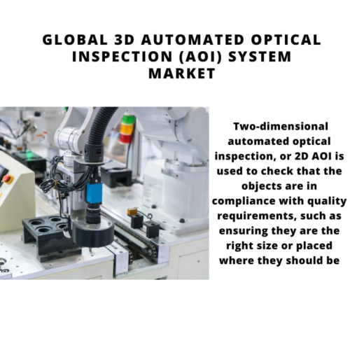
In comparison, two-dimensional automated optical inspection, or 2D AOI Typically, a camera is used to check that the objects are in compliance with quality requirements, such as ensuring they are the right size or placed where they should be.
A 3D AOI system uses side and vertical cameras to view the entire board. Because of this, 3D AOI can detect when components are reversed or skewed.
Defects including a surplus of solder joints and uneven solder can be detected by more intelligent systems. These systems depend on multi-stage lighting to give the machine vision lens enough light.
The best illumination is circular because it prevents shadows from being a potential source of erroneous calls. One advantage of 3D AOI is that it may detect flaws as small as 10 ppm. This lessens the chance of approving constructed boards when there are truly minute flaws that should lead to failure.
TheGlobal 3D automated optical inspection(AOI) system marketaccounted for $XX Billion in 2023 and is anticipated to reach $XX Billion by 2030, registering a CAGR of XX% from 2024 to 2030.
The new 3Di series of high-speed, high-precision, next-generation in-line 3D automated optical inspection (3D AOI) systems were developed by Saki Corporation, an innovator in the field of automated optical and X-ray inspection equipment, for complex inspection of high-density printed circuit boards and boards with a combination of very small and tall components.
The new 3Di series is equipped with a newly designed camera system that, by being able to concurrently and accurately check both extremely small components, such 008004s (0201 metric), and tall parts at the same time, greatly decreases cycle and provides ultra-sharp high-resolution 3D photos.
This newest automated inspection system from Saki helps to improve quality control and productivity and is ideal for high-density PCB technology inspection of the highest calibre.
| Sl no | Topic |
| 1 | Market Segmentation |
| 2 | Scope of the report |
| 3 | Abbreviations |
| 4 | Research Methodology |
| 5 | Executive Summary |
| 6 | Introduction |
| 7 | Insights from Industry stakeholders |
| 8 | Cost breakdown of Product by sub-components and average profit margin |
| 9 | Disruptive innovation in the Industry |
| 10 | Technology trends in the Industry |
| 11 | Consumer trends in the industry |
| 12 | Recent Production Milestones |
| 13 | Component Manufacturing in US, EU and China |
| 14 | COVID-19 impact on overall market |
| 15 | COVID-19 impact on Production of components |
| 16 | COVID-19 impact on Point of sale |
| 17 | Market Segmentation, Dynamics and Forecast by Geography, 2024-2030 |
| 18 | Market Segmentation, Dynamics and Forecast by Product Type, 2024-2030 |
| 19 | Market Segmentation, Dynamics and Forecast by Application, 2024-2030 |
| 20 | Market Segmentation, Dynamics and Forecast by End use, 2024-2030 |
| 21 | Product installation rate by OEM, 2023 |
| 22 | Incline/Decline in Average B-2-B selling price in past 5 years |
| 23 | Competition from substitute products |
| 24 | Gross margin and average profitability of suppliers |
| 25 | New product development in past 12 months |
| 26 | M&A in past 12 months |
| 27 | Growth strategy of leading players |
| 28 | Market share of vendors, 2023 |
| 29 | Company Profiles |
| 30 | Unmet needs and opportunity for new suppliers |
| 31 | Conclusion |
| 32 | Appendix |


© 2017-2026 Mobility Foresights Pvt Ltd. All rights reserved.
Developed with by ClousTech
