- Get in Touch with Us
Last Updated: Apr 25, 2025 | Study Period: 2024-2030
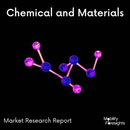
A single layer of carbon atoms organised in a two-dimensional honeycomb lattice is called graphene, and it is the source of the novel material known as graphene oxide (GO) thin film.
By oxidising graphene and adding oxygen-containing functional groups to its surface, graphene oxide is produced.This technique increases graphene's solubility and dispersibility, enabling it to be used in a variety of applications.
Due to the presence of oxygen functional groups, GO thin films have extraordinary characteristics. It has a big surface area, considerable flexibility mechanically, and great chemical stability. It is also simpler to produce and control while retaining some of graphene's electrical and thermal conductivity properties.
High surface area, mechanical flexibility, and chemical stability are just a few of the qualities that make graphene oxide thin film special. These qualities make it a flexible material with uses in biomedicine, energy storage, sensing, water purification, and optoelectronics.
GO thin films are very desirable for the development of cutting-edge technologies and gadgets due to their adaptable optical characteristics and simplicity of integration into diverse substrates. Expanding the uses and realising the full potential of graphene oxide thin films are both possible with continued research and development in this area.

The Global Graphene Oxide Thin Film Market accounted for $XX Billion in 2022 and is anticipated to reach $XX Billion by 2030, registering a CAGR of XX% from 2024 to 2030.
A new, incredibly flat monolayer graphene product has been introduced, according to Graphenea. On a substrate made of sapphire and two copper thin films, graphene is produced via CVD.
This novel product, which has a very low roughness of less than 4 nm, is intended for use in magnetic memory, freestanding membranes, high-performance electronics, and photonics.
The product's objective is to fulfil the wafer-scale integration needs for uniform graphene device construction in a way that is consistent with the most recent industrial production techniques.
The sapphire substrate is strong enough to endure mechanical damage, preventing ripping and wrinkling of the thin Cu sheet, making the flat graphene product suitable to be transferred by electrochemical delamination or dry techniques.
| Sl no | Topic |
| 1 | Market Segmentation |
| 2 | Scope of the report |
| 3 | Abbreviations |
| 4 | Research Methodology |
| 5 | Executive Summary |
| 6 | Introduction |
| 7 | Insights from Industry stakeholders |
| 8 | Cost breakdown of Product by sub-components and average profit margin |
| 9 | Disruptive innovation in the Industry |
| 10 | Technology trends in the Industry |
| 11 | Consumer trends in the industry |
| 12 | Recent Production Milestones |
| 13 | Component Manufacturing in US, EU and China |
| 14 | COVID-19 impact on overall market |
| 15 | COVID-19 impact on Production of components |
| 16 | COVID-19 impact on Point of sale |
| 17 | Market Segmentation, Dynamics and Forecast by Geography, 2024-2030 |
| 18 | Market Segmentation, Dynamics and Forecast by Product Type, 2024-2030 |
| 19 | Market Segmentation, Dynamics and Forecast by Application, 2024-2030 |
| 20 | Market Segmentation, Dynamics and Forecast by End use, 2024-2030 |
| 21 | Product installation rate by OEM, 2023 |
| 22 | Incline/Decline in Average B-2-B selling price in past 5 years |
| 23 | Competition from substitute products |
| 24 | Gross margin and average profitability of suppliers |
| 25 | New product development in past 12 months |
| 26 | M&A in past 12 months |
| 27 | Growth strategy of leading players |
| 28 | Market share of vendors, 2023 |
| 29 | Company Profiles |
| 30 | Unmet needs and opportunity for new suppliers |
| 31 | Conclusion |
| 32 | Appendix |


© 2017-2026 Mobility Foresights Pvt Ltd. All rights reserved.
Developed with by ClousTech