
- Get in Touch with Us
Last Updated: Apr 25, 2025 | Study Period:
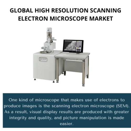
One kind of microscope that makes use of electrons to produce images is the scanning electron microscope (SEM). As a result, visual display results are produced with greater integrity and quality, and picture manipulation is made easier.
Modern research and engineering are made possible by scanning electron microscopes in a variety of fields, including medicine.
The global high resolution scanning electron microscope market accounted for $XX Billion in 2022 and is anticipated to reach $XX Billion by 2030, registering a CAGR of XX% from 2023 to 2030.
The JSM-IT700HR, a new scanning electron microscope (SEM), has been unveiled by JEOL Ltd. With a maximum probe current of 300nA and a high resolution of 1nm, the JSM-IT700HR offers a wealth of observation and analysis data.
Observation and analysis are made even simpler with a simple user interface, a small design that fits a big sample chamber, and a new anti-vibration mount for the main console.
The JSM-IT700HR adds a new feature to the SEM's graphical user interface to display the distinctive depth of X-ray generation, greatly enhancing "easy of operation."
Two new scanning electron microscopes are introduced by Hitachi High-Technologies. It has advanced automation features that make it simple to operate for both novice and seasoned operators.
These features include auto-start, wide-angle camera navigation with stitching, and auto-algorithms.
High-resolution scanning electron microscopes (SEM) are powerful tools used in various industries and research fields for imaging and analyzing the surface of samples at nanoscale resolution.
As of my last update in September 2021, I cannot provide real-time information on specific trends or which companies are currently using them. However, I can discuss four general trends that were prevalent in the high-resolution SEM industry up until that time. Please note that the landscape may have changed since then, and it's essential to refer to the latest sources for the most up-to-date information.
One significant trend in the high-resolution SEM market is the continuous improvement in resolution and imaging capabilities. Companies have been investing in research and development to enhance electron optics, detector technologies, and image processing algorithms.
This has resulted in SEMs capable of achieving atomic-scale resolution, enabling researchers to investigate and manipulate nanoscale materials and devices. These advancements have opened up new opportunities in fields such as materials science, electronics, and biology.
Another trend is the integration of SEMs with other analytical techniques. Companies have been working on combining SEM with energy-dispersive X-ray spectroscopy (EDS) and electron backscatter diffraction (EBSD) systems.
This integration allows researchers to perform chemical analysis and crystallographic characterization simultaneously with high-resolution imaging. The synergy between these techniques provides a more comprehensive understanding of the sample's composition and structure.
Automation and artificial intelligence (AI) have been making their way into high-resolution SEMs. Companies have been developing automated sample handling systems, imaging routines, and data analysis tools.
AI algorithms have been used for image processing, particle analysis, and defect recognition, making it easier for researchers to extract meaningful information from large datasets quickly. This trend has significantly improved workflow efficiency and reduced the burden on SEM operators.
Traditionally, high-resolution SEMs were large and expensive, primarily suited for dedicated research facilities and industrial labs. However, a trend that emerged in recent years is the development of compact and benchtop SEMs.
Companies have been working on miniaturizing SEM technology while maintaining respectable resolution and imaging capabilities. These smaller and more affordable systems have brought high-resolution SEM capabilities to a broader range of users, including smaller research institutions, educational settings, and industry applications.
| Sl no | Topic |
| 1 | Market Segmentation |
| 2 | Scope of the report |
| 3 | Abbreviations |
| 4 | Research Methodology |
| 5 | Executive Summary |
| 6 | Introduction |
| 7 | Insights from Industry stakeholders |
| 8 | Cost breakdown of Product by sub-components and average profit margin |
| 9 | Disruptive innovation in the Industry |
| 10 | Technology trends in the Industry |
| 11 | Consumer trends in the industry |
| 12 | Recent Production Milestones |
| 13 | Component Manufacturing in US, EU and China |
| 14 | COVID-19 impact on overall market |
| 15 | COVID-19 impact on Production of components |
| 16 | COVID-19 impact on Point of sale |
| 17 | Market Segmentation, Dynamics and Forecast by Geography, 2023-2030 |
| 18 | Market Segmentation, Dynamics and Forecast by Product Type, 2023-2030 |
| 19 | Market Segmentation, Dynamics and Forecast by Application, 2023-2030 |
| 20 | Market Segmentation, Dynamics and Forecast by End use, 2023-2030 |
| 21 | Product installation rate by OEM, 2023 |
| 22 | Incline/Decline in Average B-2-B selling price in past 5 years |
| 23 | Competition from substitute products |
| 24 | Gross margin and average profitability of suppliers |
| 25 | New product development in past 12 months |
| 26 | M&A in past 12 months |
| 27 | Growth strategy of leading players |
| 28 | Market share of vendors, 2023 |
| 29 | Company Profiles |
| 30 | Unmet needs and opportunity for new suppliers |
| 31 | Conclusion |
| 32 | Appendix |


© 2017-2026 Mobility Foresights Pvt Ltd. All rights reserved.
Developed with by ClousTech
