
- Get in Touch with Us
Last Updated: Apr 25, 2025 | Study Period: 2022-2030
The junction isolation technique works best with IC processing.
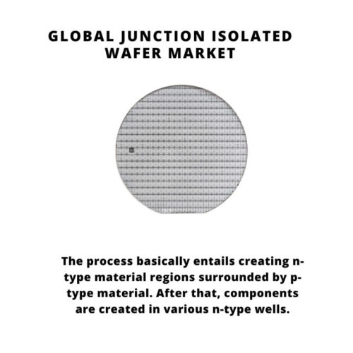
The process basically entails creating n-type material regions surrounded by p-type material. After that, components are created in various n-type wells.
Back-to-back diodes are used to electrically isolate each well and subsequently each component from the others because the p-type material surrounding the wells is given the highest negative p potential relative to all other areas of the wafer.
To prevent the unfavourable parasitic currents between the transistors, isolation between two neighbouring transistors in CMOS circuits is required for both n channel and p channel transistors.
However, because this isolation technique requires a greater amount of time than other diffusions, it takes much longer to complete.
Isolation diffusion uses a substantial amount of the chip space on the wafer surface. This space is wasted when component density is taken into account.
The performance of the circuit is harmed by the large parasitic capacitance introduced by the junction isolation method.
The Global Junction Isolated Wafer market accounted for $XX Billion in 2021 and is anticipated to reach $XX Billion by 2030, registering a CAGR of XX% from 2022 to 2030.
The launch of MEMC FOX-Si, a novel and reasonably priced silicon wafer made exclusively for offering cutting-edge FinFET technology with oxide dielectric isolation, was announced by MEMC Electronic Materials, Inc.
A "fin-based" multigate design, or FinFET, in which the conducting channel is encircled by a thin silicon "fin" constituting the body of the device, is a significant strategy for creating transistors smaller than 32 nanometers.
However, difficulties in manufacturing traditional FinFETs on bulk silicon have made it difficult to use this technology in high scale manufacturing, especially for System-On-a-Chip devices, which have significant power and cost requirements.
Junction isolation and fin dimension control, which increase unpredictability and may jeopardise scalability, are two of the main problems with FinFETS. This issue is totally eliminated by oxide separated FinFETS.
| Sl no | Topic |
| 1 | Market Segmentation |
| 2 | Scope of the report |
| 3 | Abbreviations |
| 4 | Research Methodology |
| 5 | Executive Summary |
| 6 | Introduction |
| 7 | Insights from Industry stakeholders |
| 8 | Cost breakdown of Product by sub-components and average profit margin |
| 9 | Disruptive innovation in the Industry |
| 10 | Technology trends in the Industry |
| 11 | Consumer trends in the industry |
| 12 | Recent Production Milestones |
| 13 | Component Manufacturing in US, EU and China |
| 14 | COVID-19 impact on overall market |
| 15 | COVID-19 impact on Production of components |
| 16 | COVID-19 impact on Point of sale |
| 17 | Market Segmentation, Dynamics and Forecast by Geography, 2022-2030 |
| 18 | Market Segmentation, Dynamics and Forecast by Product Type, 2022-2030 |
| 19 | Market Segmentation, Dynamics and Forecast by Application, 2022-2030 |
| 20 | Market Segmentation, Dynamics and Forecast by End use, 2022-2030 |
| 21 | Product installation rate by OEM, 2022 |
| 22 | Incline/Decline in Average B-2-B selling price in past 5 years |
| 23 | Competition from substitute products |
| 24 | Gross margin and average profitability of suppliers |
| 25 | New product development in past 12 months |
| 26 | M&A in past 12 months |
| 27 | Growth strategy of leading players |
| 28 | Market share of vendors, 2022 |
| 29 | Company Profiles |
| 30 | Unmet needs and opportunity for new suppliers |
| 31 | Conclusion |
| 32 | Appendix |


© 2017-2026 Mobility Foresights Pvt Ltd. All rights reserved.
Developed with by ClousTech
